Introduction to Photolithography
Photolithography is one of the key processes in the manufacture of computer chips. The dramatic advances in computer technology over the past few decades have been largely driven by the exponential growth in density of transistors on integrated circuits. This in turn relies on achieving smaller feature sizes during the photolithography process, by improvement in optics and by moving to lower wavelength photons. However, the semiconductor industry has reached a bottle-neck in this process and is actively embarking upon alternative technology platforms. Two of the most promising technologies for making computer chips that have feature dimensions in the order of 22 nm are 193 nm immersion lithography with double patterning and extreme UV lithography.
In immersion lithography, the space between the final projection lens and the wafer in the exposure tool is filled with water rather than air. An increase in the refractive index within this space has the effect of increasing the numerical aperture (NA) of the system (equation below), which in turn reduces the achievable feature sizes. Remarkably, computer chips that are currently being manufactured have devices with feature sizes of 45 nm using this process. Further reductions in feature size can be achieved by double patterning, which involves a more complicated set of processes, which as the name suggests involves two sequential exposures and developing steps.
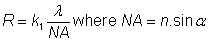
NA = numerical aperture; R= resolution; n = refractive index; λ = wavelength of light
EUV lithography uses 13.5 nm photons so can use a single patterning step to achieve 22 nm features. However, these exposures must be carried out under ultra-high vacuum which has introduced a number of technological hurdles.
Projects at UQ
- Understanding the Photodegradation of Pellicles
- High Refractive Index Photoresists for 193 nm Immersion Lithography
- Non-chemically Amplified Resists for 193 nm Immersion Lithography
- Non-chemically Amplified Resists for Extreme UV Lithography
- Advanced Lithographic Solutions using Block Copolymers: Integrating Self Assembly and Lithography